Target Support Architecture
Overview
As a separately licensed feature, the PLECS Coder can generate C code from a simulation model to facilitate embedded code generation. Plexim provides and maintains target support packages (TSPs) for specific processor families. A TSP enables the PLECS Coder to generate code that is specific to a particular hardware target such as the STM32 family of MCUs or the PLECS RT Box. With the PLECS Coder and a TSP, embedded control code can be generated, compiled, and uploaded to the target device directly from the PLECS environment with minimal effort. Furthermore, the embedded control logic can be tested extensively inside the PLECS simulation environment prior to real-time deployment.
The Embedded Code Generation Workflow
The embedded workflow is designed for you to easily transition from a PLECS model to an embedded code generation project without having to build and maintain separate models. A typical embedded code generation workflow consists of the following steps:
Design and simulate a controller and plant in PLECS. The controller represents the application that will run on the embedded target. The plant represents the hardware connected to the embedded target including the power stage and other physical systems.
Add components from the target support library to configure the embedded peripheral devices. Place the controller and peripheral models into a subsystem representing the embedded target.
Run an offline simulation. All peripheral components in the target support library have behavioral offline models to facilitate the transition from simulation to real-time deployment.
Select a discretization step size and nominal control task execution frequency. When generating C code, the PLECS Coder will use the discretization step size to automatically transform all continuous states in the controller to the discrete state-space domain using the Forward Euler method. The control task execution frequency is based on the discretization step size and specifies the nominal execution rate of the digital control loop.
Build the embedded project and flash the MCU using PLECS or the STM32CubeIDE.
Connect to the MCU using the External Mode to test the embedded control code executing on the embedded target.
Control Task Execution
Embedded applications for power electronics typically sense signals from the power converter, process the inputs using digital control laws, and output signals to actuation devices. The STM32 TSP library includes components to model and program the MCU peripherals for sensing and actuation. The control laws are implemented using standard PLECS library components.
Time synchronization of signal measurement via the analog-to-digital converter (ADC), control logic execution, and actuation via PWM outputs is critical in the digital power electronic control loop. The STM32 TSP provides the flexibility to configure the ADC and control loop interrupts through the ADC trigger and task trigger signals.
Note that there are two types of Analog In (ADC) blocks in the STM32 target library: continuous Analog In and triggered Analog In. As the name suggests, continuous Analog In block converts the selected inputs continuously. Whereas the triggered block converts the selected inputs once per trigger. The following sections use the triggered Analog In block.
ADC triggers start injected ADC conversions. The ADC start-of-conversion is driven by an event generated from a timer based component. All injected conversions associated with an ADC unit are converted sequentially when the ADC trigger is activated. The order of conversion is based on the order of the analog input channel vector. Note that regular non-triggered ADC conversions are also available.
Task triggers are generated at the end of injected conversions, PWM counter underflow and overflow events, or the Timer block events. The task trigger that connects to the Control Task Trigger component will trigger one execution of the digital control loop at the nominal base sample rate.
Additionally, the PLECS Coder and the STM32 TSP allow the user to generate multi-tasking code for the STM32 family of MCUs. For further information, refer to the Code Generation section in the PLECS Documentation. Multi-tasking code unlocks processing power for controls regulating multiple system outputs with dynamics on a range of time-scales. Using the Task Frame library component, 15 additional tasks that execute at different rates (not including the base task) can be specified, preserving processor time for the fastest, highest priority control task (base task) in the application.
Multi-tasking code generation is configured in the Scheduling tab of the Coder > Coder Options… window.
By changing the Tasking mode to multi-tasking, the sample time for each task can be configured.
The base sample time is always equal to the Discretization step size.
The Sample time setting for lower priority tasks must be an integer multiple of the base sample time.
In a multi-tasking mode, the Control Task Trigger component triggers the base task associated with the nominal base sample time.
Note
In the following sections, unless specified otherwise, control task and base task can be considered synonymous.
Control Task Accuracy and PWM Frequency Tolerance
The MCU system clock frequency, SYSCLK, fundamentally limits the time accuracy of the embedded target. SYSCLK is defined in the Target tab of the Coder > Coder Options window. The Timer and PWM carrier generation clocks are derived from an integer number of counts of SYSCLK. Therefore the time accuracy of task triggers and PWM carriers are also limited.
Consider the case where there is a desired PWM carrier frequency of \(150\,\mathrm{kHz}\) and the SYSCLK is set to \(100\,\mathrm{MHz}\). The closest achievable PWM carrier frequency is \(150.15\,\mathrm{kHz}\). Note that if the SYSCLK setting was changed to \(90\,\mathrm{MHz}\), then the target PWM frequency of \(150\,\mathrm{kHz}\) could be achieved exactly.
In cases where the PWM carrier frequency or ADC and task trigger periods cannot be achieved exactly, the default behavior is to generate an error message displaying the desired frequency or step size and the closest achievable value. Adjusting the Frequency tolerance parameter overrides this behavior and configures the PLECS Coder to automatically select the closest achievable frequency. The Frequency tolerance can be configured in the mask parameters of the Timer, PWM, and Peak Current Controller (PCC) target support library blocks.
The Discretization step size configured in the Scheduling tab of the Coder > Coder Options window will also generate an error if the exact step size cannot be achieved. This impacts the nominal period of the task trigger and introduces a numerical inaccuracy since C code derived from the model executes at a different rate than was assumed during model discretization. The Frequency tolerance parameter relating to model and control task discretization can be adjusted in the Target > General tab of the Coder > Coder Options window.
Explicit and Implicit Trigger Definitions
The interrupt sequence of the embedded application can be defined explicitly by connecting trigger signals, or implicitly where the interrupt sequence is automatically determined based on the components included in the schematic. Implicitly defined control loops will not have a Control Task Trigger component included in the schematic and all ADC trigger sources must be automatically determined. Several possible explicit and implicit trigger sequences are discussed below.
Note
Explicitly defined trigger systems require that the Control Task Trigger’s nominal base sample time parameter agrees with period of the task trigger input signal.
Control task triggered by Timer
In a basic project without an ADC or PWM component from the target support library, the task trigger must be generated by a generic Timer. The schematic below shows a simple application where a digital output is toggled at a fixed rate.
The explicit representation of the control task execution includes a Timer component that generates the input signal for the Control Task Trigger. The nominal base sample time of the Control Task Trigger must agree with the Timer task frequency. In the implicit representation the PLECS Coder will configure the Timer and Control Task Trigger automatically based on the Discretization step size parameter set in the General tab of the Coder > Coder Options… window.
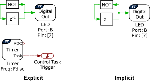
Fig. 2 Basic model with control task triggered by Timer
Control task triggered by PWM
Control task execution can be synchronized with the PWM carrier, and the repetition counter period determines how many events need to occur before a trigger is generated. When the carrier type is symmetrical, for even values of repetition counter period, the interrupts will occur at the carrier underflow or overflow events. Underflow and overflow events correspond to PWM carrier reaching the respective carrier minimum or carrier maximum values. The task trigger is configured in the Trigger tab of the PWM component.
In the explicit representation, the PWM task trigger output is connected to the Control Task Trigger component, such that execution of the digital control loop is synchronized with the PWM carrier. If the schematic does not include a Control Task Trigger or an ADC component, then the PLECS Coder will implicitly select the most appropriate source for the task trigger. First, the PWM generator that can achieve the control task frequency with the highest precision is chosen, starting from the lowest PWM number. If the control task frequency cannot be achieved exactly using a PWM carrier, then the implicit trigger logic will determine if more accurate task execution can be achieved with the Timer. The most accurate source for the control task interrupt is then selected.
The task trigger will default to triggering on underflow and overflow when the task trigger is set to disabled in the PWM Trigger tab and the trigger is implicitly defined.
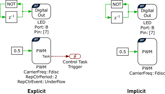
Fig. 3 Basic model with control task triggered by PWM
Control task triggered by Timer via ADC
If the schematic includes an ADC but no PWM generators, then the ADC start-of-conversion must be triggered by the Timer. In this case, the control task can be triggered by the ADC end-of-conversion or the Timer. When the ADC end-of-conversion is the source of the Control Task Trigger input, as shown in Fig. 4, then the control loop interrupt will occur after all ADC results registers are updated with the latest measurement values.
The implicit implementation automatically configures the Timer to periodically trigger the ADC start-of-conversion. The ADC trigger period is set by the Discretization step size parameter found in the Scheduling tab of the Coder > Coder Options window. The ADC unit with the greatest number of channels will trigger the control task.
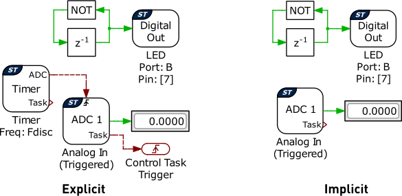
Fig. 4 Basic model with control task triggered by ADC
Control task triggered by PWM via ADC
Fig. 5 shows the explicit and implicit implementations of the control task being triggered by the ADC via the PWM. The sequence of events begins when the PWM carrier reaches an underflow or overflow triggering the start-of-conversion signal for the first ADC channel. The ADC channels are sampled and updated sequentially until the result register of the final ADC channel is updated. Once all ADC results are available, the ADC end-of-conversion interrupt triggers the control task. This arrangement synchronizes the ADC start-of-conversion with the PWM actuation and ensures the ADC results registers are updated prior to executing the control loop.
When both ADC and PWM components are included in any schematic, the PLECS Coder will implicitly select the the PWM generator with the highest control task accuracy as the ADC trigger. If the PWM generators cannot trigger the ADC at the exact target frequency, then the Timer will be used if it is more accurate. The control task will always be triggered by the ADC end-of-conversion signal.
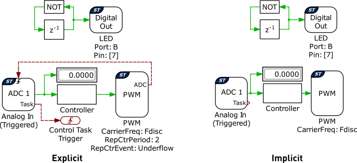
Fig. 5 Basic model with control task triggered by PWM via ADC
Advanced explicit configurations
The control task interrupt can execute at integer multiples of the PWM carrier frequency, and for a symmetric carrier the control task can be triggered at twice the PWM carrier frequency.
Fig. 6 shows a case where the discretization frequency is \(F_\mathrm{disc}\), the symmetric PWM carrier period is \(T_\mathrm{sw}=2/F_\mathrm{disc}\), and the Control Task Trigger interrupt period is \(T_\mathrm{CtrlTask}=1/F_\mathrm{disc}\). The control task is triggered twice per PWM period. Fig. 7 shows the corresponding PWM carrier, task trigger, and PWM outputs.
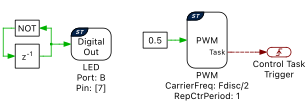
Fig. 6 PWM frequency set to half the control task frequency
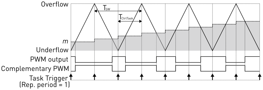
Fig. 7 PWM carrier and task interrupts for PWM frequency set to half the control task frequency
Fig. 8 shows a case where the discretization frequency is \(F_\mathrm{disc}\), the symmetric PWM carrier period is \(T_\mathrm{sw}=1/(2 \cdot F_\mathrm{disc})\), and the Control Task Trigger interrupt is generated at \(T_\mathrm{CtrlTask}=1/F_\mathrm{disc}\). Fig. 9 shows the corresponding PWM carrier, task trigger, and PWM outputs.
The STM32 TSP by default will only update the PWM duty cycle register on PWM underflow and overflow events to prevent data corruption. In Fig. 9 note the delay between the task trigger and the instant when the duty cycle, \(m\), is updated in the PWM module. The task trigger initiates the control task computation, but the modulation index is updated on the next overflow or underflow event after the entire control task has been completed. When the control task is triggered by the ADC end-of-conversion, then the modulation index will update on the next overflow or underflow event after all ADC channels are converted and the control task is completed.
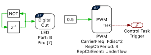
Fig. 8 Schematic of PWM frequency set to twice the control task frequency
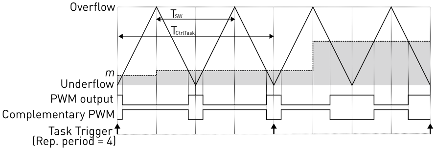
Fig. 9 PWM carrier and task interrupts for PWM frequency set to twice the control task frequency
Each ADC can receive independent start-of-conversion triggers from different PWM generators for phase-shifted sampling. Fig. 10 shows the case where the ADC1 component is triggered on the carrier overflow and ADC2 is triggered on carrier underflow from two different PWM modules with a common carrier frequency.
After all channels associated with ADC2 are converted the control task is executed with updated measurements from ADC1 and ADC2. On the next carrier overflow the PWM duty cycle register is updated.
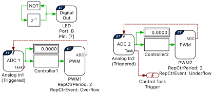
Fig. 10 Explicit phase-shifted ADC sampling
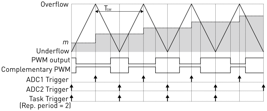
Fig. 11 PWM carrier and interrupts for phase-shifted ADC sampling
The Code Generation Project
This section provides additional technical background on the software architecture of the embedded code generation project included with the STM32 TSP.
A STM32CubeIDE project is included for each supported target chip in the projects/ folder of the TSP.
When building the project from directly from the PLECS application, the files in gcc/g4 and gcc/f3 folder of the TSP are used.
Static and dynamic code
The embedded code generation project consists of dynamic and static code. Dynamic code is generated by the PLECS Coder and is overwritten each time the Build button is clicked in the Coder > Coder Options… window. Static code is provided with the TSP and should not be modified. The PLECS Coder also generates additional dynamic configuration files that are used by the embedded application.
When the Generate code only parameter checkbox is checked, then all generated dynamic code must be placed into the ${workspace_loc}/cube_g4xx/cg or ${workspace_loc}/cube\_f3xx/cg folder of the imported STM32CubeIDE project depending on the configured target. Otherwise, by default all generated code is included in a new output directory in the same folder as the saved PLECS model.
Control and background task dispatching
The application framework includes a rate monotonic scheduler to allow precise and efficient execution of the digital control loops. The base task is executed at the highest priority. Additionally, up to 15 slower lower-priority tasks, executed at different rates, can be specified. For further information on task scheduling, refer to the Code Generation section in the PLECS Documentation. A lowest-priority background task also exists to handle non-time critical tasks. Fig. 12 shows a configuration with a base task, one additional task, and a background task executing in real-time on the MCU.
With every control task trigger interrupt issued by the Timer, PWM, or ADC end-of-conversion (bold vertical bar), any lower priority tasks are interrupted and the base task is executed. This ensures that the control task has the highest priority. In addition, the lower priority tasks are periodically triggered and executed when no higher priority tasks are active or pending.
Multi-tasking code generation is configured in the Scheduling tab of the Coder > Coder Options… window.
By changing the Tasking mode to multi-tasking the sample time for each task can be configured.
The Sample time setting for lower priority tasks must be an integer multiple of the base sample time.
The non-default tasks can be defined in the model window using the Task Frame library component.
An example of an additional LED task, along with a base PWM task is shown in Fig. 13.
Once the base and additional tasks have completed, the system continues with the background task where lowest priority operations are processed.
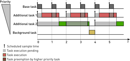
Fig. 12 Nested control tasks
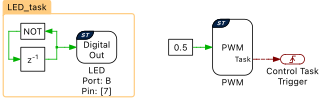
Fig. 13 Example of an additional LED task along with a base PWM task
If the base task is still executing when a second control task interrupt is received, then the processor will halt and an assertion will be generated. Similar behavior occurs if a low priority task does not complete by the time it is scheduled to execute again. If the task scheduler detects a CPU overflow and the model contains a Powerstage Protection target block, all PWM/HRTIM outputs are switched to the passive state. Assertions can be monitored using STM32CubeIDE debug tools.
Embedded project architecture
Fig. 14 shows the architecture of the embedded project included with the STM32 TSP. At the top of the software stack is an application layer consisting of the main application and the base and additional tasks. Next, there is a dispatch routine that provides a rate monotonic scheduler for the nested control tasks, as previously described. The user can choose between a custom bare-metal task scheduler or FreeRTOS™, a real-time operating system, to be used as the task scheduler. The processor-in-the-loop (PIL) framework acts as middleware for External Mode communication with the PLECS application on the user PC. The hardware abstraction layer (HAL) provides a hardware agnostic interface between the application and chip specific configuration settings. This ensures code portability between different processor platforms. The hardware specific function calls utilize the STM32 drivers to configure the MCU and key peripherals. At the bottom of the stack is the embedded hardware which includes the MCU, peripheral devices, and other onboard accessories.
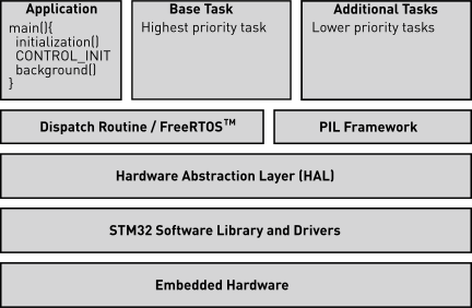
Fig. 14 Embedded project architecture