PWM
Purpose
Generate a complementary PWM signal pair
Library
STM32
Description

The PWM block generates a single or complementary PWM pair on one or more PWM resources. The modulation index for each channel must be provided via the input signal, which is a vectorized signal if the block uses multiple channels. The carrier starts at \(0\) and varies between \(0\) and \(1\). The PWM output is active when the input is greater than the carrier. The carrier frequency can be controlled by using the optional scalar input signal \(f'\). The resulting carrier frequency \(f_\mathrm{c}\) is calculated as the product of the nominal carrier frequency specified in the block parameter Carrier frequency and the input signal \(f'\). Note that all PWMs channels within one PWM block share the same frequency input.
The start of all PWM blocks is synchronized based on the same hardware trigger signal.
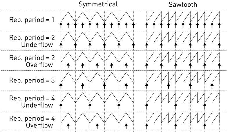
Fig. 29 Trigger events based on the repetition counter period
The PWM block can configure interrupts to trigger the ADC start-of-conversion and the Control Task Trigger. Interrupts are synchronized with the PWM carrier, and the repetition counter period determines how many events need to occur before a trigger is generated, as shown in the figure below. When the carrier type is symmetrical, for even values of repetition counter period, the interrupts will occur at the carrier underflow or overflow events. Underflow and overflow events correspond to PWM carrier reaching the respective carrier minimum or carrier maximum values.
Note
The PWM block employs preload and shadow registers to manage updates to the PWM period and modulation index. When the CPU writes a new period or modulation index value, it is first stored in a preload register. The value is then transferred to the shadow register when an update event (UEV) occurs.
The event that performs this transfer is the same event that is used to trigger the base task and is configured in the Trigger tab. It typically occurs at the end of a period or in the middle of a period and can be downsampled by a repetition counter. The TIM peripheral uses the values stored in the shadow register, ensuring that the period update takes effect only at the defined updated event.
The figure below shows an example of a symmetric PWM carrier with the repetition counter period set to \(2\), the trigger event set to underflow, and the polarity configured with an active state logic of 1.
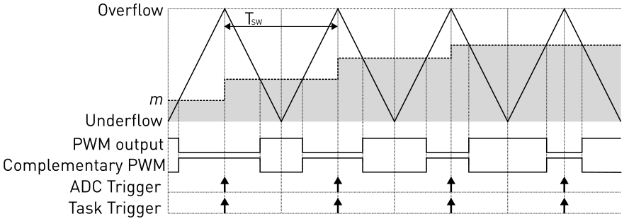
Fig. 30 PWM and trigger schemes for symmetric carrier
The PWM block protection parameters configure the break input settings for all PWM resources associated with the block. When a break input event is detected, all the PWM outputs are shutdown and are forced into the passive state.
Note
If the task scheduler detects a CPU overflow and the model contains a Powerstage Protection target block, all PWM outputs are switched to the passive state.
Parameters
Main
- TIM unit
Selects the advanced-control timer unit to use. There are two TIM units available,
TIM1,TIM8orTIM20. Each TIM unit can independently generate a single PWM output or a complementary PWM pair on up to three PWM channels.- Carrier type
Selects the carrier waveform, either sawtooth or symmetrical.
- Carrier frequency
Defines the frequency of the carrier in hertz \((\mathrm{Hz})\).
- Frequency tolerance
Specifies the behavior when the desired carrier frequency is not achievable based on the system clock frequency.
- Blanking time variation
If enabled, an additional input port d[r,f] is displayed to allow variation of the rising-edge and falling-edge delays. This port expects a vector of size 2 to set equal rising and falling delays for all channels. The units of the d[r,f] inputs are seconds \((\mathrm{s})\).
- Blanking time
Delay between the rising and falling edges of a complementary PWM output pair in seconds \((\mathrm{s})\).
- Minimal blanking time
Specifies the minimal blanking time in seconds \((\mathrm{s})\) when variable blanking time is enabled.
- Enable port
An additional component port is created if Enable port is set to value different than
Hide. If set toUse one 'En' signal per Channela singleEnsignal per channel is used and disables both PWM outputs of a channel. If set toUse one 'En' signal per PWM outputan enable signal for each PWM output has to be provided. In consequence, if a PWM channel generates a complementary signal pair the user needs to provide twoEnsignals to disable each PWM output of the same channel independently. Applying a signal \(= 0\) to this port sets the PWM channel(s) or PWM outputs to passive.- Frequency variation
Enables or disables the frequency input port \(f'\). The resulting carrier frequency \(f_\mathrm{c}\) is calculated as the product of the Carrier frequency and the input signal \(f'\).
Channel
- Mode
Configures the output PWM channel. Each TIM unit can independently generate a single PWM output or a complementary PWM pair on up to four PWM channels.
- Polarity
Defines the logical output of the PWM output when an active state is detected. The active state occurs when the modulation index exceeds the carrier.
- Port
Selects the port of the PWM output.
- Pin
Configures the pin of the PWM output.
- Complementary Port
Selects the port of the complementary PWM output.
- Complementary Pin
Configures the pin of the complementary PWM output.
Sync
- Synchronization
Specifies if the start and reset of the PWM counter should be synchronized to an external event through a External Sync block. If set to
Externala synchronization port will show up and can be connected to a External Sync block.- Trigger type
Specifies if the PWM block should react to a rising or falling edge of the external event. This parameter is only visible if the Synchronization parameter is set to
External.
Trigger
- ADC trigger
Enables or disables the ADC start-of-conversion trigger.
- Task trigger
Enables or disables the Control Task Trigger.
- Repetition counter period
Determines how many events need to occur before a trigger is generated.
- Trigger event
Selects the trigger event. When the carrier type is symmetrical, for even values of repetition counter period, the interrupts will occur at the carrier underflow or overflow events. Underflow and overflow events correspond to PWM carrier reaching the respective carrier minimum or carrier maximum values.
Protection
- Powerstage protection
Determines whether or not a Powerstage Protection block in the same PLECS model can force the PWM outputs into the passive state.
- Break input
Provides an option to configure a digital input to force shutdown all the PWM outputs associated with the block and drive them into the passive state.
Disabled: Break input is not configured.
Active low: A low voltage level on the input pin will force the PWM outputs into the passive state. If the input voltage transitions from the low level to the high level, the PWM output signal will resume.
Active high: A high voltage level on the input pin will force the PWM outputs into the passive state. If the input voltage transitions from the high level to the low level, the PWM output signal will resume.
- Break input port
Selects the digital input port to be configured as the break input.
- Break input pin
Configures the digital input pin to be configured as the break input.