Peak Current Controller
Purpose
Implement peak current control with ramp compensation
Library
STM32
Description
The Peak Current Controller (PCC) block implements peak current control with slope compensation.
In a peak current-mode controller, at the beginning of each switching cycle the output is set (gate signal is turned ON) without a pre-determined duty cycle. Then, when the sensed inductor current exceeds the peak current reference value, the output is reset (gate signal is turned OFF). The duty cycle is therefore determined by the rise of the inductor current during the on-time.
One of the drawbacks of the peak current-mode controller is that it suffers from an inherent instability if the applied PWM duty cycle is greater than \(50\,\%\). This is explained in the figure titled “Slope compensation”. If a small disturbance is introduced into the system and if the applied duty cycle is less than \(50\,\%\), the disturbance eventually decays to zero. However, if the applied duty cycle is greater than \(50\,\%\), the inductor current will start to diverge and will no longer be stable. The resulting duty cycle values will vary from small to large, on an alternating cycle basis, called sub-harmonic oscillations. To limit these sub-harmonic oscillations, instead of providing a constant peak current reference, additional slope compensation is applied, which then ensures the stability of the inductor current.
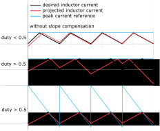
Fig. 24 Slope compensation
Internally, the PCC block makes use of multiple MCU peripherals. The first component is a DAC that provides a peak current set-point including ramp, for controlling the inductor current. The second is a comparator (COMP); the sensed current is fed to the comparator, which is then compared to the peak current set-point provided by the DAC. The output of the COMP block is fed to the third component, which is the high-resolution timer (HRTIM). The HRTIM generates the PWM waveforms and synchronizes the DAC at the specified frequency.
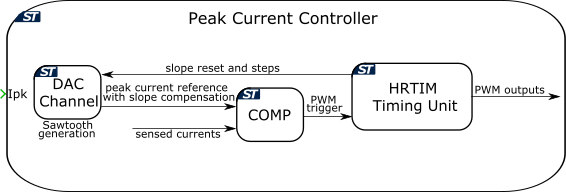
Fig. 25 Peak current controller schematic
The peak current reference \(I_\mathrm{pk}\) is provided as an input to the PCC block. Logic is included in the PCC block such that when \(I_\mathrm{pk} = 0\), all associated PWM outputs are driven into the passive state.
The Peak Current Controller block can also be used as burst mode controller. Burst mode operation is commonly used during light load conditions to increase the converter efficiency. It allows to have the output channels alternatively in idle and run state, by hardware. Due to this, some switching periods can be skipped with configurable periodicity and variable duty cycle. The burst mode duty cycle can be set by the \(Bd\) input terminal and has to be a value between \(0\) and \(1\).
Parameters
Main
- High resolution timer unit
Selects the high resolution timer (HRTIM) unit to use. There are two HRTIM units available. Each HRTIM unit can independently generate a single PWM output or a complementary PWM pair on up to three PWM channels.
- Switching frequency
Defines the switching frequency of the output signal in hertz \((\mathrm{Hz})\).
- Frequency tolerance
Specifies the behavior when the desired carrier frequency is not achievable based on the system clock frequency.
- Current sense scale
Scales the peak current reference \(I_\mathrm{pk}\) into values with physical units \((\mathrm{V/A})\) to be used for the control algorithm.
- Ramp slope
Defines ramp slope rate in amperes per second \((\mathrm{A/s})\). Slope compensation can be applied to ensure stability when the output duty cycle exceeds \(50\,\%\). Entering a parameter, \(I_\mathrm{ramp}\), reduces \(I_\mathrm{pk}\) during each switching cycle as follows: \(I_\mathrm{pk}' = I_\mathrm{pk} - I_\mathrm{ramp}\cdot t\), where \(t\) is the time elapsed from the start of the switching cycle. Slope compensation can be omitted by setting \(I_\mathrm{ramp}\) to 0. On chips of the F3 target family, slope compensation is not supported and has to be omitted by setting the ramp slope to zero.
- Ramp offset
Defines ramp offset in amperes \((\mathrm{A})\).
- Leading edge blanking time
This sets the minimum output on time at the beginning of each switching period in seconds \((\mathrm{s})\). Leading edge blanking time is used to prevent the turn-on transient current from triggering the peak current controller.
Channel
- Mode
Configures the output PWM channel. Each HRTIM unit can independently generate a single PWM output or a complementary PWM pair on up to three PWM channels.
- Sense port
Selects the port of the sensed current.
- Sense pin
Configures the pin of the sensed current.
- Timing unit
Selects the HRTIM unit of the output channel. HRTIM timing unit
Fis not available on chips of the F3 target family.- Output Polarity
Defines the logical output of the PWM output when an active state is detected. The active state occurs when the sensed current exceeds the peak reference current set-point.
- Switching blanking time
Specifies the delay between the rising and falling edges of a complementary PWM output pair in seconds \((\mathrm{s})\).
Burst mode
- Burst mode
Enables or disabled the burst mode controller.
- Burst mode frequency
Defines the burst mode periodicity in hertz \((\mathrm{Hz})\). This parameter is only visible if Burst mode is
Enabled.