Powerstage Protection
Purpose
Provide powerstage safety features
Library
STM32
Description

The Powerstage Protection block implements an interlock, which is a safety mechanism, to enable or disable all the PWM outputs on the target device. The PWM outputs are disabled unless there is a logical low to high transition on the input signal, labeled en. This prevents the PWM signals from becoming active as soon as the code is executed on the target, thereby ensuring safe operation.
Additionally, there is an option to configure a digital output as a powerstage enable signal. This signal can then be used, for example, to provide an enable signal to external gate driver chips. The enable polarity of the digital output, specified in the Powerstage enable pin can be defined as:
Active low: a logical low to high transition on the input signal, en, sets the digital output pin to logic low (
0).Active high: a logical low to high transition on the input signal, en, sets the digital output pin to logic high (
1).
To reiterate, the powerstage enable signal (GPIO out) is an output signal of the Powerstage Protection block. This signal does not contribute to enabling or disabling PWM outputs, and can be considered as a status indicator of the Powerstage Protection interlock state. Irrespective of the configuration of this signal (Digital output or None), the Powerstage Protection block, if included in the schematic, disables all the PWM outputs on the target device, unless there is a logical low to high transition on the input signal, labeled en.
When the PWM outputs are disabled via the Powerstage Protection input, all associated PWM outputs are driven into the passive state. If the task scheduler detects a CPU overflow and the model contains a Powerstage Protection target block, all PWM/HRTIM outputs are switched to the passive state as well.
If the Powerstage Protection block is omitted from the schematic, then all PWM outputs will be continuously enabled.
Protection
- Analog protection signals
Each analog protection signal can be configured in the Target > Protections tab of the Coder > Coder Options… window to emit up to seven specific trip signals (labeled
1-7). When a trip signal is detected, the Powerstage Protection module can take no action (Ignore) or activate a one-shot trip event (Disable powerstage (one-shot)). A one-shot trip event will disable the powerstage by setting the outputs of all PWM blocks to the inactive state and HRTIM outputs to the state defined in the channel fault state parameter of the HRTIM Timing Unit block. All trip events are latched and can only be cleared by cycling the Powerstage Protection block from disabled to enabled.
Timing
When the Powerstage Protection en input is activated, the digital output (GPIO out) associated with the block (if configured) will immediately become active to e.g. enable a gate driver chip. However, the actual PWM signals will remain disabled for \(100\,\mathrm{ms}\) to allow the gate driver circuit to stabilize. During this period the signal output of the Powerstage Protection block will remain low. Only at the end of the \(100\,\mathrm{ms}\) delay will the signal output transition to high, simultaneously with the PWM signals becoming active. Therefore, a regulator reset or anti-windup mechanism must be controlled by the output signal of the Powerstage Protection block (signal out), and not the en input.
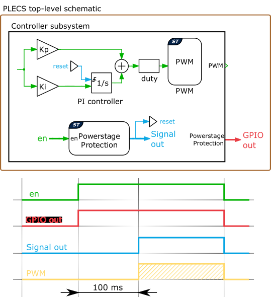
Fig. 26 Powerstage Protection timing
Parameters
Main
- Powerstage enable signal
Provides an option to configure a digital output as a powerstage enable signal.
Digital output: Configures a digital output as a powerstage enable signal. This signal can then be used, for example, to provide an enable signal to external gate driver chips. This signal can be considered as a status indicator of the Powerstage Protection interlock state.
None: Powerstage enable signal is not configured.
- Powerstage enable polarity
Defines the polarity of the powerstage enable signal.
Active low: a logical low to high transition on the input signal, en, sets the GPIO pin to logic low (
0).Active high: a logical low to high transition on the input signal, en, sets the GPIO pin to logic high (
1).
- Powerstage enable port
Selects the digital output port to be configured as the powerstage enable signal.
- Powerstage enable pin
Defines the digital output pin to be configured as the powerstage enable signal.
- Powerstage enable pin output characteristic
Specifies whether an internal pull-pull or open drain resistor is connected to the digital output.
Protection
- Reaction to analog protection signal 1-7
Selects the action following an analog trip event detection. The Powerstage Protection can take no action (
Ignore) or activate a one-shot trip event (Disable powerstage (one-shot)) as reaction to an analog protection signal.
Offline only
- Interlock
For convenience, the interlock can be enabled or disabled for offline simulations.
Select Simulate to enable the simulation of the interlock safety mechanism. The output of the the Powerstage Protection block in the top-level schematic is disabled unless there is a logical low to high transition on the input en.
Select Do not Simulate to disable the simulation of the interlock mechanism. The output of the the Powerstage Protection block can then be enabled at the start of the simulation by tying en to 1.
Note
Note that the offline model of the Powerstage Protection block only simulates the powerstage interlock mechanism, in conjunction with the block output and the Powerstage enable signal digital output.
The effect that the Powerstage Protection block has on the individual PWM signals is not represented in an offline simulation, and needs to be separately implemented by the user. An example is shown in the figure below. The Powerstage enable signal digital output is wired to a PWM enable/disable Signal Switch, thereby simulating the enable signal of a gate driver circuit.
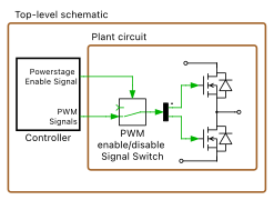
Fig. 27 An offline implementation of the gate driver logic of the Powerstage Protection block