SPI Master
Purpose
Implement SPI Master connected to one or multiple slaves
Library
STM32
Description

The Serial Peripheral Interface (SPI) is a high-speed synchronous serial input/output device that allows a serial bit stream of programmable length (4 to 16 bits) to be shifted into and out of the device at a configurable bit-transfer rate. The SPI is usually used for communications between the MCU controller and external peripherals, or another controller.
The SPI is a master-slave based interface with a single master and one or more slave devices.
The interface consists of the following signals:
MISO Serial data input (master in/slave out)
MOSI Serial data output (master out/slave in)
SCK Shift-clock, generated by the SPI Master
/CS Chip-select or slave-select signal. The chip-select signal is an active-low signal that enables the MISO and MOSI ports of the SPI Slave.
The SPI Master block provides a clock signal (SCK) which generates a configurable number of clock pulses during each simulation step. For both the slave and the master, data is shifted out of the shift registers on one edge (rising or falling) of the CLK and latched into the shift register on the opposite clock edge. If the clock phase (CPHA) bit is configured to 1, data is transmitted and received a half-cycle before the SCK transition.
Multiple SPI Slaves can be supported by a single master through chip-select (/CS) signals. The figure below shows an example of a single SPI Master with two SPI Slaves.
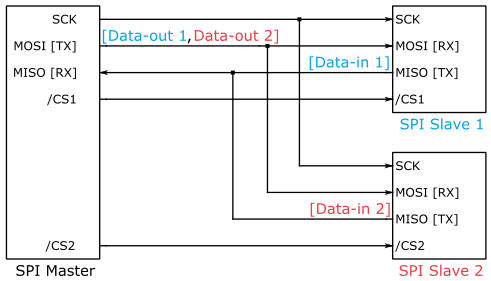
Fig. 31 SPI Master with two SPI Slaves
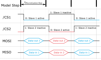
Fig. 32 An example of signal exchange between one SPI Master and two SPI Slaves
The SPI Master block exchanges data with only one SPI Slave block per block execution step. If there are multiple slaves, then data is exchanged over multiple steps. For example, as illustrated in the figure above, during the first step, the master enables SPI Slave 1 using the chip-select signal and transmits Data-out 1; at the same time the master also receives Data-in 1 from the first slave. During the second step, after enabling SPI Slave 2, the master transmits Data-out 2 and receives Data-in 2 from the second slave simultaneously. This process then repeats.
An output value of \(1\) at the v port indicates that valid data is sent to all the slaves.
The data to be transmitted is provided at the input TX and the data received is available at the output RX.
TX: For transmitting data to multiple slaves, provide a vector with a length equal to the sum of the number of words per transmission per each slave. For example, in the figures above, if Data-out 1 is a packet of 4 words [1,2,3,4] and Data-out 2 is a packet of 3 words [16,17,18], then the input to the TX block is provided as a vector of 7 words [1,2,3,4,16,17,18].
RX: Similarly, data from multiple slaves is received as a vector with a length equal to the sum of the number of words per transmission per each slave. For example, in the figures above, if Data-in 1 is a packet of 4 words [21,22,23,24] and Data-in 2 is a packet of 3 words [36,37,38], then the output of the RX block is read as a vector of 7 words [21,22,23,24,36,37,38].
If the SPI Master does not have enough time to complete the transmission before the block is executed again, the output o turns 1 to indicate an overrun error.
If an overrun error is being signaled at the o port of the SPI Master, it is possible that the task with which the SPI Master is associated executes too fast. In this case, either reduce the SPI Master execution task rate or increase the SPI clock rate.
For example, if SCK is set as \(180000\,\mathrm{Hz}\), and is expected to transmit a packet of 4 words at 8 bits per word, then the time it would take to transmit one packet is
In this case, the execution step size of the SPI Master must be set to values greater than \(0.178\) milliseconds.
Parameters
Setup
- SPI module
Selects the SPI module to use.
- SPI clock
Defines the SPI clock frequency (SCK), also known as the SPI Baud Rate, in hertz \((\mathrm{Hz})\). If the SPI clock frequency cannot be hit accurately, a warning is issued during code generation. Please refer to the STM32 technical reference for more information on the range of achievable SPI clock rates.
- Bits per word (4-16)
Defines the length of a single data word during transmission. The allowed length is 4 to 16 bits per word.
- Mode [CPOL, CPHA]
Defines four SPI clocking modes, controlled by clock polarity (CPOL) and clock phase (CPHA) bits. CPOL controls whether the clock signal is high (1) or low (0) when idle. CPHA controls whether data is shifted in and out on the rising or falling edge of the clock signal. The following table summarizes ST’s convention of clock polarity and phase according to the standard SPI operating modes:
Table 1 SPI Clocking Modes Mode
CPOL
CPHA
SPI Clock Scheme
SPI_MODE0
0
0
Rising edge without delay
SPI_MODE1
0
1
Rising edge with delay
SPI_MODE2
1
0
Falling edge without delay
SPI_MODE3
1
1
Falling edge with delay
- Offline simulation
Enables or disables data inspection in an offline simulation. If set to enable, terminals are added to the subsystem in the top-level schematic. If set to disable, no such terminals are added to the subsystem.
GPIO Settings
- SCK Port
Selects the port name of the clock frequency signal.
- SCK Pin
Defines the pin number of the clock frequency signal.
- MISO Port
Selects the port name of the MISO signal.
- MISO Pin
Defines the pin number of the MISO signal.
- MOSI Port
Selects the port name of the MOSI signal.
- MOSI Pin
Defines the pin number of the MOSI signal.
Slave(s)
- CS Port
Selects the port name to use for chip-select. In a multi-salve setup, all individual chip-select signals must be assigned to the same port group.
- CS Pin(s)
Defines the pin number of the chip-select signal. Any GPIO can be configured to be a chip-select signal. Provide a vector to configure multiple slaves.
- Words per transmission (vector for multiple slaves)
Configures the number of transmitted data words in each simulation step. Provide a vector to configure multiple slaves.