Full-Bridge Inverter
Purpose
Full-bridge voltage source inverter with filter inductance, optimized for Real-Time Simulations on the RT Box.
Library
Electrical / Nanostep
Description
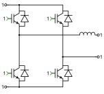
This component implements a full-bridge voltage source inverter including a filter inductor on the AC side.
Both sides of the converter have current source behavior. The DC side must be connected directly to a capacitor or a voltage source.
The component offers two configurations:
Nanostep / SwitchedThe power semiconductors are modelled as ideal switches controlled by instantaneous logical gate signals. A switch is turned on when the corresponding gate signal is
true.In
Nanostep / Switchedconfiguration, C code generated from this component is suitable for real-time simulations on the RT Box, where it is executed on a Nanostep solver. In this case, connect the gate inputs to PWM Capture blocks from the RT Box component library.The Nanostep implementation requires the DC and AC sides to be galvanically isolated. Any electrical connection between the two sides outside the component would therefore not reflect the actual current and voltage situation and should be avoided.
Sub-cycle averageEach gate input is controlled by a floating-point number with values between \(0\) and \(1\), representing the relative on-time of the corresponding semiconductor over one simulation step, as described in Sub-cycle Averaging.
In
Sub-cycle averageconfiguration, C code generated from this component is suitable for real-time simulations on the RT Box, where it is executed on the CPU or FlexArray solver. In this case, connect the gate inputs to PWM Capture blocks from the RT Box component library.
Note
This component has a Nanostep solver weight of \(1\), indicating that it occupies \(\frac{1}{3}\) of a Nanostep solver for Real-time Simulations on the RT Box.
Note
The voltage sources connected to the converter must not be short-circuited. Therefore, combinations of switching signals that cause shoot-through of DC links are not permitted. Additionally, DC voltages across diodes must not be negative, as DC voltage clamping through diodes is not permitted.
Parameters
- Configuration
Selects the component configuration. See the descriptions of
Nanostep / SwitchedandSub-cycle averageabove.- Switch model (CPU code generation)
If the Configuration is set to
Sub-cycle average, this parameter selects the switch model when CPU code is generated.- Semiconductor symbol
Use this setting to choose between
IGBTandMOSFETfor the symbol of the active semiconductor switches. This setting only affects the schematic representation and does not change the electrical behavior of the component.- Inductance
A non-zero scalar specifying the inductance \(\mathrm{L}\), in henries \((\mathrm{H})\).
- Winding resistance
A scalar specifying the winding resistance \(\mathrm{R_L}\), in ohms \((\Omega)\).
- Assertions
When set to
on, the block flags an error for combinations of gate signals that cause shoot-through.
Nanostep Probe Signals
See Fig. 267 for the probe signal positions.
- Inductor current
The current through the inductor \(\mathrm{L}\), in amperes \((\mathrm{A})\), defined positive in the direction of the arrow.
- DC link current
The current at the DC-link side converter terminals, in amperes \((\mathrm{A})\), defined positive in the direction of the arrow.
- Gate signals
A vector containing the gate signals of the active semiconductor switches.
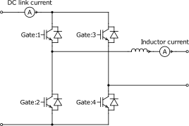
Fig. 267 Probes for the Full-Bridge Inverter
↳ Added in PLECS 4.9.