Matrix CLLLC Converter
Purpose
CLLLC converter with 1/2/3/4-phase matrix converter frontend, optimized for Real-Time Simulations on the RT Box.
Library
Electrical / Nanostep
Description
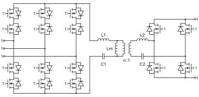
This help page applies to a set of components implementing isolated, resonant CLLLC converters with a 1-, 2-, 3-, or 4-phase matrix front-end. The topology can be configured as a dual active bridge (DAB) by omitting the resonant capacitors, or as an LLC converter by omitting the secondary-side inductor and capacitor.
Both sides of the converter have current source behavior and must each be connected directly to a capacitor or a voltage source.
The power semiconductors are modelled as ideal switches controlled by instantaneous logical gate signals. A switch is turned on when the corresponding gate signal is true.
C code generated from this component is suitable for real-time simulations on the RT Box, where it is executed on a Nanostep solver. In this case, connect the gate inputs to PWM Capture blocks from the RT Box component library.
Note
This component has a Nanostep solver weight of \(3\), indicating that it occupies one entire Nanostep solver for Real-time Simulations on the RT Box.
Note
Inductive currents must not be interrupted abruptly. Therefore, at all times, the combination of switch signals on the matrix front-end must provide a path for the inductive current of the primary winding. This can be achieved by ensuring that at least one high-side switch and one low-side switch are simultaneously ON in the direction of the current flow.
The voltage sources connected to the converter terminals must not be short-circuited. Therefore, combinations of switching signals that cause phase-to-phase short circuits or shoot-through conditions are not permitted. Additionally, DC voltages across diodes must not be negative, as DC voltage clamping through diodes is not permitted.
Parameters
Certain parameters are associated with specific components. The corresponding component labels such as \(\mathrm{L}\), \(\mathrm{C}\), etc., are shown in Fig. 275.
- Primary inductance
A non-zero scalar specifying the primary-side inductance \(\mathrm{L_1}\), including the transformer leakage inductance and any external series-connected inductor, in henries \((\mathrm{H})\).
- Primary winding resistance
A scalar specifying the primary-side winding resistance \(\mathrm{R_{L1}}\), in ohms \((\Omega)\).
- Include primary capacitor
Allows you to include (
yes) or remove (no) a resonant capacitor at the primary side.- Primary resonant capacitance
If the Include primary capacitor option is set to
yes, this parameter requires a non-zero scalar for the capacitance \(\mathrm{C_1}\), in farads \((\mathrm{F})\).- Magnetizing inductance
A non-zero scalar specifying the magnetizing inductance of the transformer \(\mathrm{L_m}\), referred to the primary side, in henries \((\mathrm{H})\).
- Include secondary inductance
Allows you to include (
yes) or remove (no) a series leakage inductance on the secondary side.- Secondary inductance
If the Include secondary inductance option is set to
yes, this parameter requires a non-zero scalar specifying the secondary-side series inductance \(\mathrm{L_2}\), including the transformer leakage inductance and any external inductors, in henries \((\mathrm{H})\).- Secondary winding resistance
If the Include secondary inductance option is set to
yes, this parameter requires a scalar specifying the secondary-side winding resistance \(\mathrm{R_{L2}}\), in ohms \((\Omega)\).- Include secondary capacitor
Allows you to include (
yes) or remove (no) a resonant capacitor at the secondary side.- Secondary resonant capacitance
If the Include secondary capacitor option is set to
yes, this parameter requires a non-zero scalar for the capacitance \(\mathrm{C_2}\), in farads \((\mathrm{F})\).- Turns ratio
A scalar specifying the ratio of primary-side turns to secondary-side turns.
- Assertions
When set to
on, the block flags an error for combinations of gate signals that cause shoot-through or interruption of inductive currents.
Probe Signals
See Fig. 275 for the probe signal positions.
- Inductor currents
A vector containing the currents through the inductors \(\mathrm{L_1}\) and \(\mathrm{L_2}\), in amperes \((\mathrm{A})\), defined positive in the direction of the arrow.
- Magnetizing current
The current through the inductor \(\mathrm{L_m}\), in amperes \((\mathrm{A})\), defined positive in the direction of the arrow.
- Capacitor voltages
A vector containing the voltages across the capacitors \(\mathrm{C_1}\) and \(\mathrm{C_2}\), in volts \((\mathrm{V})\), defined positive at the sides marked with (+).
Nanostep Probe Signals
- Inductor currents
A vector containing the currents through the inductors \(\mathrm{L_1}\) and \(\mathrm{L_2}\), in amperes \((\mathrm{A})\), defined positive in the direction of the arrow.
- Magnetizing current
The current through the inductor \(\mathrm{L_m}\), in amperes \((\mathrm{A})\), defined positive in the direction of the arrow.
- Primary currents
A vector containing the currents at the primary-side converter terminals, in amperes \((\mathrm{A})\), defined positive in the direction of the arrow.
- Secondary current
The current at the secondary-side converter terminals, in amperes \((\mathrm{A})\), defined positive in the direction of the arrow.
- Capacitor voltages
A vector containing the voltages across the capacitors \(\mathrm{C_1}\) and \(\mathrm{C_2}\), in volts \((\mathrm{V})\), defined positive at the sides marked with (+).
- Primary gate signals
A vector for each phase containing the gate signals of the primary-side semiconductor switches.
- Secondary gate signals
A vector containing the gate signals of the secondary-side semiconductor switches.
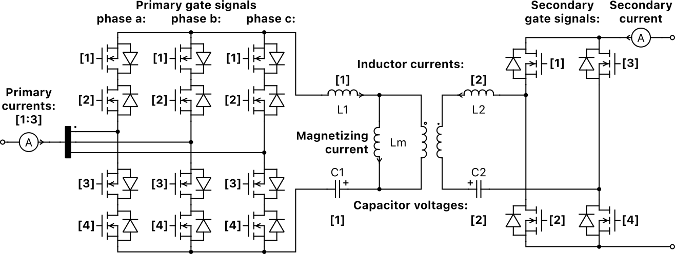
Fig. 275 Probe Signals for the 3x1 Matrix CLLLC Converter
↳ Added in PLECS 5.0.